

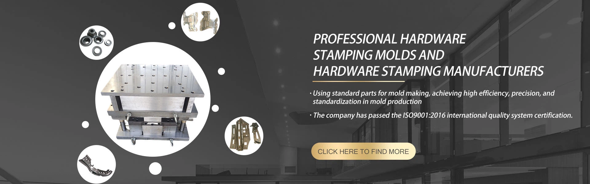


The rapid miniaturization of modern consumer tech, smart appliances, and telecommunication devices demands an unprecedented level of micro-precision. At the core of this hardware revolution is the Electronics Stamping Die, a specialized manufacturing tool engineered to produce ultra-thin, highly complex metal components at hyper-high speeds.
Unlike heavy industrial automotive tooling, electronic stamping focuses on micron-level tolerances, intricate geometric details, and the gentle handling of highly conductive raw materials. Whether your production line outputs micro-connectors, semiconductor lead frames, or shielding cans, our tooling ensures zero-defect repeatability across hundreds of millions of cycles.
Architectural Breakdown of Micro-Precision Electronic Tooling
To achieve consistent accuracy when working with foil-thin metals, the internal architecture of the tool must be built to completely different standards than standard mechanical dies.
[Precision Coil Feeder] ➔ [Micron-Level Carrier Indexing] ➔ [In-Die Carbide Punching] ➔ [Integrated Vision Inspection]
Sub-Micron Punch and Die Clearances: When stamping materials as thin as 0.05 mm, the clearance between the punch and the matrix must be perfectly uniform to prevent burrs, edge deformation, or material pulling.
Solid Carbide Segment Architecture: To prevent wear under continuous high-speed friction, all critical cutting, bending, and forming inserts are machined from premium sub-micron tungsten carbide grades.
Modular Segmented Inserts: The entire tool is split into sub-assemblies. If a single micro-punch wears out, operators can swap out a single insert block within minutes directly on the press, without dismantling the entire die set.
Technical Performance Parameters
The following technical indexing illustrates the precision control boundaries applied during our engineering and manufacturing processes:
Plaintext
[Material Thickness Range] 0.03 mm to 1.50 mm (Ultra-Thin Foil to Medium Strip) [Machining Tolerances] Wire EDM and Profile Grinding accuracy down to ±0.002 mm [Die Set Material] High-rigidity alloy steel plates with pre-loaded ball guide posts [Target Raw Materials] Beryllium Copper, Phosphor Bronze, Brass, Nickel Alloys, SUS304 [Production Speed Limits] High-speed press operations ranging from 200 to 800 Strokes Per Minute (SPM) [Secondary Automation] In-die tapping, contact-riveting, and multi-track terminal forming
Addressing the Strict Requirements of Electronic Procurement
Electronic components must maintain flawless signal integrity and mechanical fit. Our engineering methodology directly counters the most common failure points in precision electronics production.
We eliminate plating peel and micro-cracking by designing specialized bending radii that match the grain direction of sensitive alloys like phosphor bronze. This is crucial for battery contacts and spring terminals that require long-term elasticity.
To protect delicate parts from catastrophic deformation, our tools feature high-pressure, mirror-polished stripper plates that hold the strip perfectly flat during the entire cutting and lifting cycle. This ensures that even the most complex electromagnetic shielding (EMI) cages remain flat and ready for automated surface-mount technology (SMT) pick-and-place lines.
Furthermore, we integrate automated optical fiber sensors directly into the die structure to monitor strip alignment and part ejection in real time. If a scrap slug fails to drop, the sensor instantly stops the high-speed press, protecting your valuable carbide inserts from double-stamping damage.
Partner with a Micro-Tooling Authority
Manufacturing a high-speed Electronics Stamping Die requires a perfect blend of advanced tool design, premium materials, and elite grinding craftsmanship. Our engineering team conducts full strip layout simulations to optimize material utilization, directly lowering your precious metal scrap costs.
Connect with our engineering desk today to submit your product designs, material specifications, and annual volume requirements. We will provide a comprehensive design feedback analysis and an industrial commercial quotation within 48 hours.
Hot Tags: ultra-precision electronics stamping die for high-density component manufacturing, China ultra-precision electronics stamping die for high-density component manufacturing manufacturers, suppliers, factory, Anti climbing nail stamping die, Compound Die Stamping, Construction stamping die, Kitchenware stamping die, Piercing Die, Sheet Metal Stamping


